IC packaging complexity levels are rising year-by-year in lock step with process advances and electrical performance enhancements. Single die packages with leads have given way to multi-chip area array packages, stacked die packages, and stacked packages. Pin-counts have increased from a few handfuls to thousands. Space constraints for consumer products have required shrinking some packages to barely larger than the chip volume, and high-performance applications have required ever increasing levels of power dissipation and higher frequency operation. Pin count increases and wide I/O have driven substrate technologies to include upwards of 20 or 30 interconnect layers. Higher integration levels in automotive applications have motivated higher reliability requirements. At the same time, time-to-market and cost reduction requirements have forced an ever-accelerating product development pace where missing a product launch can spell a company’s doom. Trial and error iteration won’t work in today’s industry.
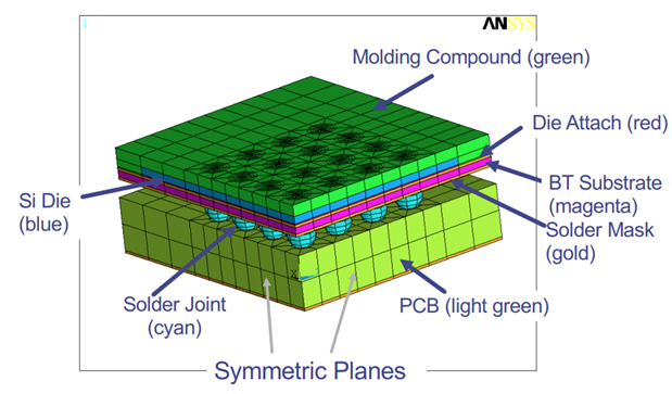
The only way to meet the interrelated demands of complexity, performance, time-to-market, and reliability is through appropriate package design processes and modeling. IC Packaging Design and Modeling is an 8 hour course that covers fundamental issues in package design, including the need for appropriate risk analysis, up-front design rules, early look-ahead, and modeling coupled with verification. Compact models that enable transferring phenomenological behavior between die, package, and system level models will be described. Mechanical analysis examples applied to a wide range of reliability issues will be emphasized with a focus on solving issues in advance.