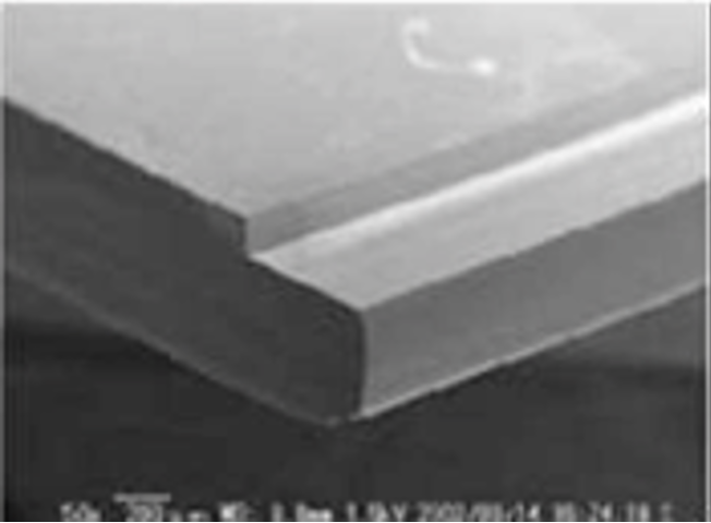
This course provides a detailed overview of wafer backgrinding, a crucial process for wafer thinning and enabling 3D stacking technologies. We'll begin by discussing the importance of wafer thinning for stacking applications. The course will then delve into the mechanics of backgrinding, differentiating between ductile and brittle grinding and their respective damage profiles. You'll learn about crack formation during backgrinding and methods for preparing samples to view these backside cracks. Furthermore, we'll explore techniques for strengthening thinned silicon wafers and the necessity of temporary bonding to support fragile wafers during processing. The course will cover temporary bonding processes, including UV debonding and edge trimming, as well as the materials used and their characterization. Finally, we'll examine various wafer bonding and debonding technologies, including mechanical and laser ablation methods, and discuss the challenges of thin die pick and place.